


Fiber Optic Tech
Understanding Optical Chips and Their Applications
Optical chips are fundamental components that enable the conversion of electrical signals into optical signals and vice versa. Their performance directly determines the transmission efficiency of optical communication systems. Optical communication systems utilize light pulses as information carriers and optical fibers as the transmission medium. Information is transmitted using optical signals through a process of electrical-to-optical conversion. In optical communication systems, the transmitter side employs laser chips to convert electrical signals into optical signals, which are then transmitted via optical fibers to the receiver side. At the receiver side, detector chips convert the optical signals back into electrical signals. Optical chips play a crucial role in determining the transmission speed and network reliability of various network systems, including fiber access, 4G/5G mobile communication networks, and data centers.
Functional Classification of Optical Chips
Optical chips can be categorized into two main types based on their function: laser chips and detector chips. Laser chips are primarily used to generate optical signals by converting electrical signals into light pulses. Detector chips, on the other hand, are responsible for receiving optical signals and converting them back into electrical signals.
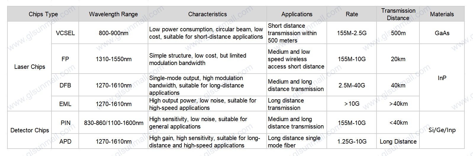
Laser chips can be further classified into two types based on their light emission structure: surface-emitting chips (VCSEL) and edge-emitting chips. Edge-emitting chips include Fabry-Perot (FP), distributed feedback (DFB), and external-cavity modulation (EML) lasers.
VCSEL (Vertical-Cavity Surface-Emitting Laser) Chips: These chips emit light perpendicular to the surface of the chip. They are widely used in data centers for short-distance communication due to their high-speed capabilities and low power consumption.
FP (Fabry-Perot) Chips: An early form of laser chip, FP chips are used for low-speed, short-distance transmission. They function by allowing light to resonate within a cavity, producing a coherent output.
DFB (Distributed Feedback) Chips: These chips incorporate a grating filter within the laser cavity to produce a single longitudinal mode output, making them suitable for high-speed, medium, and long-distance transmission.
EML (Electro-absorption Modulated Laser) Chips: EML chips integrate a DFB laser with an electro-absorption modulator, enhancing signal quality and enabling high-speed, long-distance transmission by mitigating dispersion issues.
Detector chips are primarily categorized into PIN and APD detectors.
PIN (Positive-Intrinsic-Negative) Diodes: These diodes operate by generating photogenerated carriers when light photons strike the semiconductor material. The photogenerated current is then converted into an electrical signal.
APD (Avalanche Photodiode) Chips: APDs enhance the signal through an avalanche multiplication process, wherein photogenerated carriers are accelerated in a high-field region, causing secondary ionization and resulting in a significant increase in photocurrent. Although APDs provide high sensitivity and efficiency, they are prone to higher noise levels.
Classification Based on Raw Materials
Optical chip manufacturers typically employ III-V compound semiconductors, such as indium phosphide (InP) and gallium arsenide (GaAs), as the substrate materials for their chips. These materials possess advantageous properties, including high frequency response, excellent performance under extreme temperature conditions, low noise, and strong radiation resistance, making them well-suited for high-frequency communication applications.
Indium Phosphide (InP) Substrate: InP is used to fabricate FP, DFB, and EML edge-emitting laser chips, as well as PIN and APD detector chips. These chips are primarily employed in telecommunication and data center applications involving medium-to-long-distance transmission.
Gallium Arsenide (GaAs) Substrate: GaAs is used to fabricate VCSEL surface-emitting laser chips. These chips are primarily employed in short-distance data center applications and 3D sensing applications.
Detector chips are fundamental components in optical communication systems, responsible for converting optical signals into electrical signals. This conversion is based on the principle of the photoelectric effect, which states that when a material is exposed to light, electrons within the material absorb the energy of photons. If the absorbed energy exceeds the material's work function, the electrons will escape the material, forming photoelectrons, and leaving behind positively charged holes.
PIN Detectors: PIN detectors operate through a two-step process: Photon Absorption and Charge Generation. Photons incident on the semiconductor material generate light-generated carriers (electron-hole pairs). Current Generation and Signal Output: Under the influence of an external circuit, the light-generated current flows, producing an electrical signal that is subsequently output.
APD Detectors: Avalanche photodiodes (APDs) differ from PIN detectors in that they incorporate an avalanche region within their basic structure. This avalanche region enables the collision ionization effect, where light-generated carriers in the avalanche region generate new electron-hole pairs through impact ionization. The newly generated carriers are accelerated by the electric field, leading to further impact ionization, resulting in an avalanche multiplication of the light-generated current. Consequently, APDs offer the advantages of high output power and high efficiency. However, they also exhibit higher noise levels compared to PIN detectors.
Detector chips play a crucial role in optical communication systems, enabling the conversion of optical signals into electrical signals, which can then be processed and interpreted by electronic devices. The two main types of detector chips, PIN and APD, each have their own advantages and disadvantages, making them suitable for different applications within optical communication systems.
Technical Principles of Optical Chips
Laser Chips: Electrical-to-Optical Conversion.The fundamental principle of laser chips involves the conversion of electrical energy into optical energy through electrical excitation. Semiconductor materials serve as the gain medium, and the injected electrical current is stimulated, leading to the emission of laser light through optical resonance amplification and mode selection. The gain medium and substrate are primarily composed of doped III-V compound semiconductors, such as GaAs (gallium arsenide), InP (indium phosphide), and Si (silicon-based) materials.
Laser chip optical designs can be categorized into two main types based on their resonance cavity fabrication process: edge-emitting laser chips (EEL) and surface-emitting laser chips (VCSEL). EELs employ optical coatings on both sides of the chip to form a resonance cavity. Photon amplification occurs through resonance cavity mode selection, resulting in laser emission parallel to the substrate surface. VCSELs, on the other hand, employ optical coatings on both the top and bottom surfaces of the chip to form a resonance cavity. Since the resonance cavity is perpendicular to the substrate, photon amplification occurs through mode selection, resulting in laser emission perpendicular to the chip surface.
EELs are further classified into FP, DFB, and EML lasers. FP and DFB lasers are independent devices that modulate the output laser signal by controlling the presence or absence of current. These lasers are known as directly modulated laser (DML) chips. FP lasers, with their simple structure and low cost, are primarily used for low-speed, short-distance transmission. DFB lasers, built upon the FP laser design, employ a grating filter to achieve single-mode output, making them suitable for high-speed, medium-to-long-distance transmission.
Applications of Optical Chips
Optical chips are integral to a wide range of applications, driving advancements in various fields:
Telecommunications: Optical chips enable high-speed data transmission over long distances in telecommunications networks. DFB and EML laser chips, along with PIN and APD detector chips, are commonly used in fiber optic communication systems to ensure reliable and efficient signal transmission.
Data Centers: In data centers, VCSEL chips are widely used for short-distance, high-speed data transmission between servers and storage devices. The high bandwidth and low power consumption of VCSELs make them ideal for the dense interconnect environment of data centers.
Mobile Communication Networks: The deployment of 4G and 5G mobile networks relies heavily on optical chips to handle the increased data traffic and higher speeds. Laser and detector chips facilitate the rapid and efficient transmission of data between base stations and network nodes.
Sensing and Imaging: Optical chips are also used in sensing and imaging applications, such as 3D sensing in smartphones and automotive LiDAR systems. The precise control and high-speed capabilities of VCSELs make them suitable for these applications, where accurate distance measurement and imaging are critical.
Future Trends and Developments
The evolution of optical chips is driven by the continuous demand for higher data rates, lower power consumption, and greater integration. Key trends and developments in the field include:
Integration with Silicon Photonics: The integration of optical chips with silicon photonics aims to combine the high-speed capabilities of optical chips with the scalability and cost-effectiveness of silicon-based electronics, paving the way for more compact and efficient optoelectronic devices.
Advancements in Material Science: Ongoing research into new materials, such as compound semiconductors and novel nanostructures, promises to enhance the performance and efficiency of optical chips, enabling higher data rates and broader wavelength ranges.
Quantum Communication: Optical chips are expected to play a crucial role in the development of quantum communication networks, where they will facilitate the transmission of quantum information over long distances with high security.
Artificial Intelligence and Machine Learning: The integration of optical chips with AI and machine learning technologies holds potential for optimizing network performance, improving signal processing capabilities, and enabling real-time data analysis in various applications.
Optical chips are vital to the functionality and advancement of modern communication systems. Their ability to efficiently convert and transmit signals underpins the high-speed, reliable data transmission essential for telecommunications, data centers, mobile networks, and beyond. As technology continues to evolve, optical chips will remain at the forefront of innovation, driving progress in communication and sensing technologies and shaping the future of our interconnected world.


