


Fiber Optic Tech
Introduction to Laser Chips and Packaging
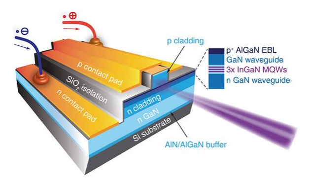
Laser chips are the core components of modern optoelectronic technology, and their material systems determine the performance and application areas of lasers. According to different material systems, laser chips are mainly divided into gallium nitride (GaN)-based blue light series, gallium arsenide (GaAs), indium phosphide (InP), etc. These materials usually exist in the form of ternary or quaternary compounds, and have their own unique characteristics and application advantages.
Gallium nitride (GaN) is a wide bandgap semiconductor material that is widely used in blue lasers due to its excellent electron mobility and high thermal conductivity. GaN-based lasers have the characteristics of high power, high efficiency and long life, and are widely used in fields such as optical disc reading, display technology and medical equipment.
Gallium arsenide (GaAs) is an important III-V semiconductor material that is widely used in lasers in the infrared and near-infrared bands. The GaAs material system can be combined with elements such as aluminum and antimony to form a variety of compounds, such as aluminum gallium arsenic (AlGaAs) and indium gallium arsenic (InGaAs). These materials are widely used in electro-optical communications, optical storage and radar technology.
Indium phosphide (InP) is a material that plays a key role in long-wavelength optical communications. InP can be combined with elements such as indium, gallium, and aluminum to form a variety of alloys, such as indium gallium arsenic phosphide (InGaAsP). These alloys have excellent performance in the 1.3 micron and 1.55 micron bands and are ideal materials for optical fiber communications.
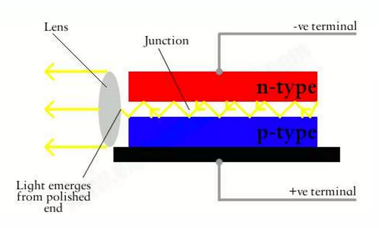
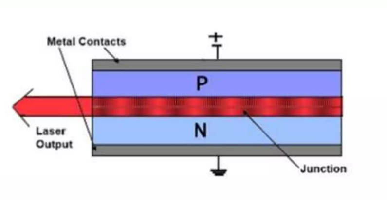
Laser chips are composed of GaN-based blue light series, gallium arsenide, indium phosphide and other ternary or quaternary systems according to the material system. Each material system has different optimal epitaxial substrates, and the directions of gold wires on the P and N sides are also different. These differences are reflected in the electrode design, including the arrangement direction of the positive and negative electrodes, which may be in the same direction or in the opposite direction.
Choice of Epitaxial Substrate
GaN-based lasers often use sapphire (Sapphire) or silicon carbide (SiC) as substrates.
GaAs-based lasers often use GaAs or Ge (germanium) substrates.
InP-based lasers use InP substrates.
Electrode Design
Positive and negative electrodes are arranged in the same direction: it simplifies the packaging and electrical connection design, and is often used in high-power lasers.
Positive and negative electrodes are arranged in opposite directions: it is suitable for specific structural requirements and optimizes device performance.
According to the scope of use, laser chips are mainly divided into visible light for high-power applications, infrared light for communication, and 800~980nm infrared light for medical beauty. There are significant differences in the size of chip designs based on the power requirements of different applications. For example, laser chips for high-power applications usually have larger lengths and widths to provide higher output power and better heat dissipation performance, and the width of their light-emitting bands is also wider; infrared laser chips for communications tend to Due to the miniaturized design, the length and width are smaller, and the light-emitting band is narrower to meet the needs of high-speed data transmission; the laser chip for medical beauty uses a balance of power and precision in terms of length, width, and light-emitting band width to ensure the accuracy of treatment. Effectiveness and safety.
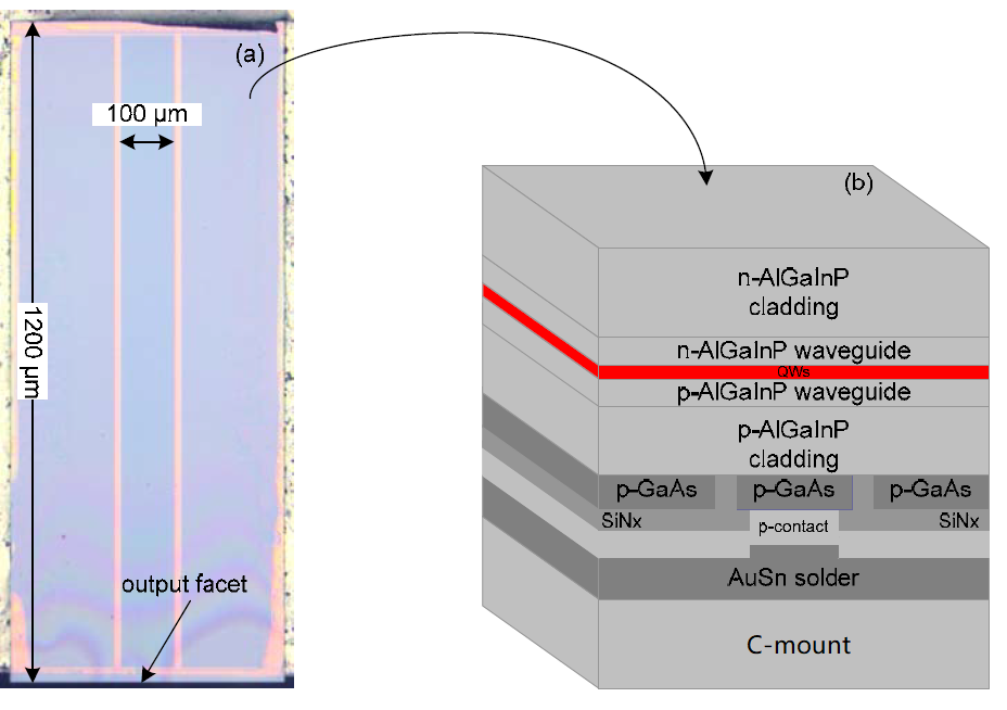
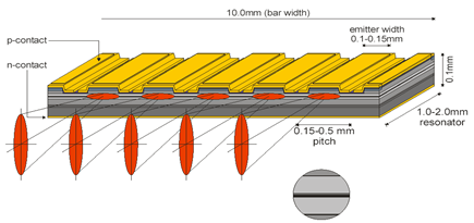
For high-power lasers, a longer resonant cavity length is required, and 1000um or more is common. For low-power communication lasers, 100um is generally sufficient, as shown in the figure below.
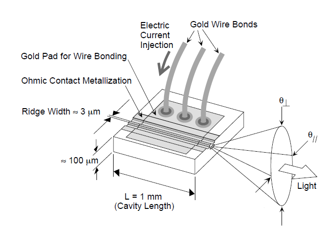
The pad diameter of the gold wire is generally around 80um, so the wire bonding position needs to be specially designed for small chips.
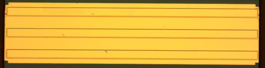
At the same time, multiple light strips can be designed on a chip according to needs. There can be as many as needed, which is also called chip-level integration. The advantage is that the light power of chips of the same size is much greater. The disadvantage is that the heat dissipation requirements are high.
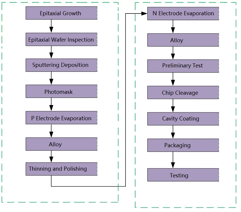
Chip Production Process
The preparation process of laser chips is a highly precise and multi-step process, which usually includes key steps such as epitaxial growth, lithography, etching, metallization and packaging. First, semiconductor layers are grown on epitaxial substrates by molecular beam epitaxy (MBE) or chemical vapor deposition (CVD) technology. These layers determine the basic performance of the chip. Next, the required pattern is formed on the semiconductor layer using photolithography, and then the excess material is removed by plasma etching or wet etching technology to form precise circuits and structures. The metallization process involves depositing a conductive metal layer on the chip to form electrodes and interconnections. Finally, after testing and sorting, the chip is packaged into a housing suitable for its application to ensure good performance and reliability in practical applications. Each step needs to be carried out in a clean room environment to avoid contamination and defects to ensure the high quality of the final product.The laser made into wafer needs to be dissociated into bars first, and then the bars are stacked and coated.
Laser Chip Packaging
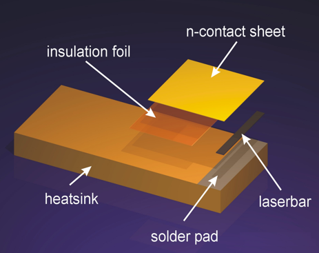
In order to obtain a laser with higher power and better heat dissipation, people often use a whole bar to package the laser.
Calculated based on 2W per light-emitting unit and 1um×100um active area, the body heat density is 2×10¹⁰W/m3. Calculated based on 50% electro-optical conversion efficiency, a typical medium power of 50W/bar, a cavity length of 1mm, a heat flux density of 500W/cm2, and a current density of 1000A/cm2.
Therefore, in order to achieve the best heat dissipation effect, the P surface needs to be facing down and in direct contact with the heat sink. Because the active area is closer to the P surface, the distance between the active area and the P surface is generally within 200nm, and the distance to the N surface is about 90um. Therefore, in order to allow the heat to be transferred to the heat sink over a shorter distance, the heat sink is made the positive electrode and the upper surface is made the negative electrode.
Single-tube laser chips can be packaged in various ways to meet diverse application requirements and working environments. The main packaging methods include TO-can, C-mount, and Q-mount, each offering unique characteristics and advantages.
TO-can Packaging
TO-can packaging (Transistor Outline) is a traditional and widely used method. It employs a metal shell to fully enclose the laser chip, providing excellent mechanical protection and thermal management. TO-can packaging is known for its low cost, simple process, and high reliability. The typical structure includes a metal base where the laser chip is welded, and a metal cap is sealed in a vacuum environment to create a fully enclosed structure. This packaging is ideal for high-power and high-reliability applications such as optical communication, laser ranging, and laser printing.
TO packaging technology, namely Transistor Outline or Through-hole packaging technology, is a fully enclosed packaging method with the advantages of low cost and simple process. In this technology, the chip is first soldered to the TO base to ensure that it is fixed and the electrical contacts are connected. Next, a metal cap is put on to completely enclose the chip to provide mechanical protection and environmental isolation. This process needs to be carried out in a vacuum environment to prevent air and moisture from entering the package to ensure the long-term stability and reliability of the chip. TO packaging can not only effectively prevent the influence of the external environment on the chip, but also achieve good heat dissipation, making it widely used in various high-reliability and high-power electronic and optoelectronic devices, such as power transistors, laser diodes and sensors.
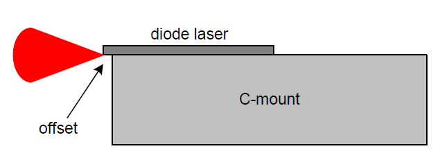
C-mount Packaging
C-mount packaging is an method where the laser chip is mounted on a metal base with a heat sink and without a fully enclosed shell. This design offers superior heat dissipation as the chip is directly exposed to air or an external heat sink. C-mount packaging is often used in laboratory environments and high-power laser applications that require efficient heat dissipation and easy adjustment. Its simple structure makes it easy to install and disassemble, making it suitable for laser performance testing and adjustment.
Q-mount Packaging
Q-mount packaging is similar to C-mount but features a more compact and modular design. The laser chip in a Q-mount package is mounted on a small metal base, typically equipped with precision alignment and fixing mechanisms to ensure accurate and stable optical alignment. This packaging is suited for applications requiring precise alignment and high stability, such as precision measuring instruments and high-precision optical communication equipment.
The choice of packaging method primarily depends on specific application requirements and environmental conditions:
TO-can Packaging: Best for applications requiring high reliability and fully enclosed protection.
C-mount Packaging: Ideal for applications needing efficient heat dissipation and convenient adjustment.
Q-mount Packaging: Suitable for applications requiring high precision and stability.
Each packaging method has unique advantages and applications, ensuring the laser chip performs optimally in various scenarios.
In summary, single-tube laser chips can be packaged in diverse ways. TO-can, C-mount, and Q-mount packaging each offer distinct features that cater to different application needs, ensuring the laser chip performs at its best in various optoelectronic devices.


